Our Solutions
Silicon Photonics
We provide enhanced foundry services for silicon photonics through a dedicated 8” commercial fab with intellectual property (IP) and know-how to convert customer design into reality.
Our Capabilities
CompoundTek converts customer design into end products through our own proprietary silicon photonics manufacturing process and dedicated 8” CMOS foundry (<90nm-180nm). Our dedicated fab supports fast turn-around full reticle field or Multi Project Wafers (<2 months depending on number of mask layers) and high-volume mass production requirements.


Our Technology
Silicon photonics continues to be a leading technology enabler in data communications, making possible faster interconnects with highr-density optical connectivity for 100Gbe, 400Gbe, 800Gbe and beyond. The demand today comes from data centers that require solutions to move data faster and more efficiently. CompoundTek’s Silicon Photonics fabrication technology & PDK support customers towards achieving these goals. Other applications supported by our technology include biomedical sensing, LIDAR, optical interconnectivity, artificial intelligence & machine learning and high performance computing. CompoundTek enables companies to fabricate their silicon photonic ICs using our proprietary Process Design Kit and production-proven fabrication process. All the basic passive and active silicon photonics building blocks for Multi-Project Wafer (MPW) and standalone product runs are available on our platform for our customers to validate their designs.
- Si waveguides (Rib, Strip and grating couplers) with 193nm ArF lithography enabling 90nm minmum geometry.
- Low Loss SiN waveguides.
- TiN heater and ion implantation-doped Silicon heater for thermal tuning.
- Six ion implantations (N, N+, N++, P, P+, P++) for modulators
- Ge photodetectors (lateral, vertical NIP and vertical PIN)
- Tungsten Plug contacts, 3 metal layer process with ultra thick Cu Metal 1 and 2 and thick Aluminium Metal 3
- Cladding oxide etch, isotropic Silicon etch and DRIE Deep Trench Silicon etch for suspended and non-suspended coupler options
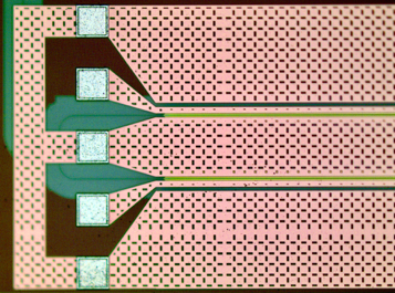
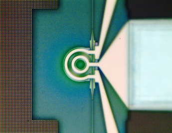
Some of the silicon photonics active and passive photographs, are shown below:


In addition, CompoundTek has a complete silicon photonics electro-optic and testing capability.
The design rule of each layer is specified in the process design kits (PDK). The PDK content covers the following:
- Si photonics full stack schematics
- Design rule (DR)
- Si photonics mask Graphic Database System (GDS) layers
- Mask tape-out process flow
- Max MPW and full reticle field size restriction
- Design rule check (DRC)
- Basic Si photonics design blocks GDS examples (Si waveguide, SiN waveguide, grating coupler, fiber edge coupler, vertical Ge photodetector, Mach-Zehnder interferometer (MZI) modulator, etc.)
Next Generation SiPh
In collaboration with our research partners, CompoundTek has embarked on next generation transceiver development (400G/lane & above) by incorporating Lithium Niobate into a SiPh-TFLN heterogenous integration platform.