Monolithically integrated optical isolator chips with sputter-coated Ce:YIG films on silicon waveguides
SEUNG HWAN KIM1,3,4, BEOMSU PARK1, JI WOON PARK1, HYO‑SEUNG PARK1, JUYEONG MOON1, SUNG HYEON JANG1, RAMADAS NAMBATYATHU2, ROBIN CHAO2, S GUNASAGAR2, HAN-YOUL RYU3,5, AND KYONG HON KIM1*
1PhotoniSol Inc. 30 Songdomirae-ro, Songdo-Smartvalley B422, Incheon, 21990 Republic of Korea 2CompoundTek, Pte Ltd., 5 International Business Park, 609914, Singapore 3Department of Physics, Inha University, Incheon 22212, Republic of Korea4 shkim@photonisol.com, 5hanryu@inha.ac.kr* kyongh@photonisol.com
Abstract: This paper presents an experimental demonstration of monolithically integrated optical isolator chips with sputter-coated Ce:YIG films on silicon waveguides, using the nonreciprocal phase shift effect of a Mach-Zehnder-type interferometer. A fully CMOScompatible optical isolator chip has been developed, achieving 27.7 dB of optical isolation and 6.4 dB of insertion loss at an input wavelength of 1550 nm. The isolator chip has an area of 220 × 1310 m² and can be readily integrated with other silicon photonic devices to enable complete photonic integrated-circuit applications. This initial result indicates that monolithically integrated optical isolators, produced via mass-producible sputtering to deposit MO films directly on silicon waveguides, are feasible for large-scale manufacturing. Additionally, chip performance can be further enhanced by optimizing waveguide structures and magneto-optic film-coating conditions. The high-temperature annealing processes commonly used to crystallize MO films can be replaced by localized laser annealing.
1. Introduction
Optical isolator chips are essential components of photonic integrated circuits (PICs), ensuring stable operation of the laser source by preventing back-reflected light from interrupting the laser and enabling proper optical signal processing. Complementary metal-oxidesemiconductor (CMOS)-compatible optical isolator chips are particularly important when various laser diodes, optical amplifiers, modulators, and multiplexing devices are integrated together to protect optical signal transmitters, ensure the stable flow of the laser beam in the intended direction, and properly control the flow of optical signals in desired directions by blocking unwanted leakage.
Various technical approaches have been demonstrated for developing integrated optical isolators, beginning with initial ideas for waveguide-type optical isolators [1,2]. Physical principles utilizing optical nonlinearity [3,4], photonic crystals [5], temporal modulation [6,7], optomechanical and acoustics[8 ‒10], non-Hermitian parity-time symmetry [11], and magnetooptic effect [12‒32] were used to demonstrate waveguide-type optical isolator chips. However, integrated schemes using magneto-optic (MO) films on silicon waveguides are the most promising for practical applications due to their energy-efficient, passive photonic-device performance [15‒32]. Two main approaches to MO-film-based optical isolator chips involve the nonreciprocal polarization rotation (NPR) and nonreciprocal phase shift (NPS) effects [1,2]. Integrated optical isolator chips built on silicon optical waveguides that utilize the NPR effect face difficulties with phase-matching conditions between the transverse-electric (TE) and transverse-magnetic (TM) polarization modes in planar waveguide structures. This results in very strict fabrication error margins, making NPR-based optical isolator chip manufacturing challenging and limiting achievable performance [12‒15]. NPS-based optical isolator chips that use optical interferometer structures have been considered easier to produce, and device performance has been demonstrated by research groups worldwide. Silicon waveguide-based optical isolator chips of micro-ring resonator (MRR), Mach-Zehnder interferometer (MZI) and multimode interferometer (MMI) types have been demonstrated with a magneto-optic film cladding, either by bonding or pulsed-laser deposition (PLD) of Ce:YIG films [16‒33]. In recent studies, a monolithic integration method for Ce:YIG films directly on silicon or silicon nitride waveguides using pulsed laser deposition (PLD) has been reported [21], demonstrating the feasibility of implementing high-performance optical isolators without wafer bonding. The PLD method is considered unsuitable for mass-production film coating in conventional CMOS processes.
The sputtering method is widely used in conventional CMOS processes for thin-film deposition. Sputtered europium-substituted cerium iron garnet (Ce:EuIG) films have been used in MRR-type isolator chips [31], but neither Ce:YIG nor Ce:EuIG films have been used in MZItype isolator chips. MRR-type isolator chips have an extremely narrow isolation bandwidth and are highly sensitive to environmental conditions, thereby limiting their practical use. By contrast, MZI-type isolator chips have a relatively wider isolation bandwidth and are less sensitive to environmental conditions.
In this paper, we present an experimental demonstration of MZI-type optical isolator chips based on the NPS with directly sputtered Ce:YIG films on silicon waveguides. These chips can be manufactured relatively easily using standard CMOS processes and sputter-deposited magneto-optic films on silicon waveguides. It will be demonstrated that our isolator chips achieved an optical insertion loss of 6.4 dB and an isolation of 27.7 dB, with a footprint of 220 × 1310 m². Details of the device structures and the experimental results will be provided in the following sections.
2. Device concept and operating principle
In this research, we have focused on demonstrating MZI-type optical isolator chips based on the NPS, with directly sputtered Ce:YIG films on silicon waveguides. These chips can be manufactured relatively easily using standard CMOS processes and sputter-deposited magnetooptic films on silicon waveguides. The device scheme and optical microscope image of the isolator chip are shown in Fig. 1. It consists of two 1 × 2 multi-mode interferometers (MMIs) for input and output coupling ports of an MZI, which includes an NPS section with the MO cladding on each arm and a reciprocal phase shift (RPS) section on one arm. Grating couplers (GCs) are formed for input and output beam couplings. The total chip dimensions are 220 m in width and 1310 m in length, excluding the GCs, where the MO section length is 1000 m.
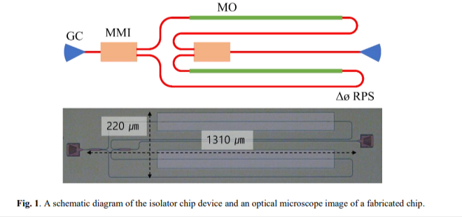
2.1 Nonreciprocal phase shift (NPS)-based optical isolator
The optical isolator chip is designed to operate on the basis of the optical interferometer characteristics of the NPS effect in a silicon waveguide with an MO cladding. A forward beam passing through the chip undergoes constructive interference at the opposite output port due to the accumulated phase shift through the NPS and RPS sections, while the reverse beam experiences destructive interference from the accumulated phase shift. A key feature of our devices is the use of monolithically coated MO cladding directly on the silicon waveguides, fabricated by sputtering. Unlike MO film bonding or pulsed laser deposition (PLD), sputtering can be easily adapted to conventional CMOS and mass-production processes. Key technical challenges include the formation of high-quality, low-loss MO films on silicon waveguides to achieve the required optical isolator chip characteristics.
2.2 TM mode operation and NPS mechanism
The isolator chip was designed and analyzed to exploit the NPS characteristics of TM-polarized beams. For TM-mode beams, the electric-field component is distributed upward along the waveguide, enabling interaction with the MO film on the top cladding. This structural geometry induces the NPS effect on the propagating beam along the silicon-core waveguide via magnetooptical effects within the MO film. Figure 2(a) shows a cross-sectional schematic of the silicon waveguide and MO film cladding used in this study. An MO film was directly deposited onto the silicon waveguide by sputtering, and the stacked structure was designed to allow the TM-mode field to overlap with the MO film. A cross-sectional scanning electron microscope (SEM) image of the fabricated waveguide structure is shown in Fig. 2(b), confirming that the MO film was uniformly deposited on the silicon waveguide. A SEM image of the deposited MO film surface shown in Fig. 2(c) indicates that the sputtering process provides a continuous and uniform morphology of the MO films deposited on silicon wafers. Figure 2(d) is a top-view SEM image of the MO
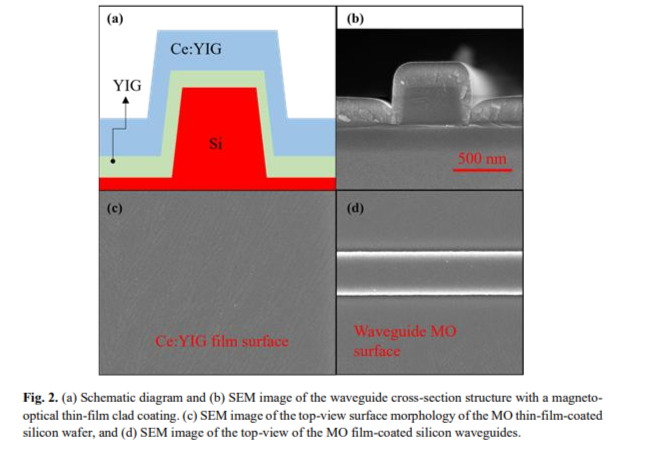
film deposited directly on the silicon waveguides, confirming that the film was properly formed along the waveguide pattern.
The isolator chip exploits the NPS effect of two oppositely propagating TM-mode beams when an external magnetic field is applied perpendicular to the beam propagation. The phase shift accumulates along the waveguide propagation distance and is proportional to the Faraday rotation characteristics of the MO film cladding, the mode confinement factor in the clad region, and the waveguide geometry. In the following section, we numerically analyze the NPS characteristics by accounting for these factors and verifying the validity of the optical isolator design.
3. Waveguide design and numerical simulation
In this section, we numerically analyze the optical mode characteristics of a silicon waveguide clad with a sputter-coated MO film and calculate the magnitude of the NPS for a TM-mode beam propagating along the waveguide. We evaluate the TM-mode profile and beam confinement factor within the MO thin film as a function of the waveguide geometry. Based on these results, we design a suitable optical isolator chip structure.
3.1 Silicon waveguide geometry and mode analysis
We considered silicon waveguides fabricated on silicon-on-insulator (SOI) wafers with a cerium-substituted yttrium iron garnet (Ce????Y3−????Fe5O12, Ce:YIG) MO film deposited on the cladding. As reported in previous publications, a yttrium iron garnet (YIG) film was first deposited on top of the silicon waveguide as a buffer layer to alleviate the lattice mismatch between the silicon wafer and Ce:YIG film. The SOI wafer had a top-silicon thickness of 350 nm and a 2-m-thick buried oxide (BOX) layer. The waveguide width was set to 450 nm, which ensures stable TM-mode propagation in the 1.5-m optical communication wavelength range
while also providing sufficient electromagnetic field overlap within the upper MO film. Numerical analysis was performed by calculating the eigenmodes in the waveguide crosssection, and the mode profile was analyzed for the TM mode. In the numerical simulation, a Faraday rotation (FR) value of 200 deg/cm was applied to the YIG buffer layer, while that of −3000 deg/cm was applied to the upper Ce:YIG film. These settings ensured that the Ce:YIG layer predominantly induced the NPS effect.
3.2 TM-mode profile and confinement in YIG and Ce:YIG films.
The TM-mode beam profiles were calculated in the silicon core waveguide, the YIG buffer, and the Ce:YIG MO clad films to determine the mode confinement factor in the MO films, as shown in Fig. 3. The silicon core waveguide had a thickness of 350 nm and a width of 450 nm.
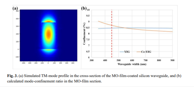
The YIG buffer layer had a thickness of 30 nm, and the Ce:YIG MO film layer had a thickness of 200 nm. The calculated results show that the TM-mode confinement in the YIG layer is 8.5%, while the upper Ce:YIG layer exhibits 8.7% mode confinement. Similar levels of mode confinement were observed in both layers, indicating that the optical mode is effectively distributed throughout the magnetic thin-film stack. Since the FR value of the YIG film is much smaller than that of the Ce:YIG films, the upper Ce:YIG layer plays a dominant role in the formation of NPS. Therefore, the subsequent analysis of NPS characteristics focuses on the magneto-optical properties of the Ce:YIG layer.
3.3 Simulated NPS and phase accumulation
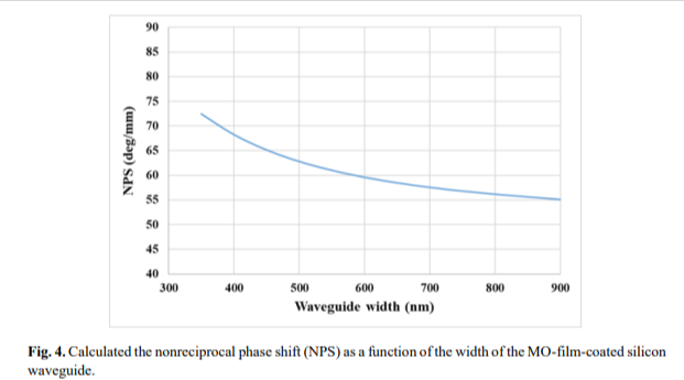
To quantitatively assess the NPS induced in the silicon waveguide with the Ce:YIG MO clad film, we calculated the NPS per unit length for the TM-mode beam. The NPS was derived from the difference in propagation constants along the propagation direction under an applied external magnetic field perpendicular to the beam propagation, and the phase accumulation characteristics along the waveguide length were also analyzed. The calculated results are shown in Fig. 4 as a function of waveguide width. The calculated NPS per unit length is approximately 65 deg/mm when the waveguide width is 450 nm. This indicates that the phase accumulation
required for 90-degree operation in the MZI-type optical isolator is achievable even at relatively short propagation lengths. As shown in these numerical analysis results, this study confirmed that a silicon waveguide structure integrated with sputtered YIG and Ce:YIG thin films can provide sufficient phase characteristics for implementing NPS-based optical isolators. In the following sections, we fabricate a device based on these design results and experimentally verify the optical isolator’s performance.
4. Device fabrication and material characterization
This section describes the process flow for an optical isolator fabricated on a silicon photonics platform and the characteristics of the MO film deposited by sputtering. The silicon waveguide was fabricated using standard commercial foundry processes, and subsequent process steps optimized MO film deposition and thermal treatment conditions to achieve non-reciprocal optical transmission.
4.1 Device fabrication on a silicon photonics platform
The starting material was 200 mm diameter SOI wafers with a 350 nm thick top silicon layer on a 2 μm thick buried oxide layer. A 3-mask layer process was used to fabricate the waveguide layers, including grating couplers, rib and strip waveguides. This process was adapted from an existing production silicon photonics process used at the foundry, with necessary recipe adjustments to minimize development effort.
An initial 10 nm thick thermal oxidation stress relief layer was formed, followed by a 100- nm-thick low-pressure chemical vapor deposition (LPCVD) silicon nitride (Si3N4) layer. This Si3N4 layer was used as a hardmask to etch 40-nm-deep trenches for grating couplers and partial etches of rib and strip waveguides. The lithography step to etch the Si3N4 hardmask and silicon was performed on a dry 193 nm ArF scanner capable of a minimum feature size of 65 nm. The use of ArF lithography, rather than conventional Deep UV (DUV) lithography for the 1st mask layer, improved silicon sidewall roughness, resulting in reduced optical scattering. To ensure a silicon loss of 40 nm thickness, the etch time was calibrated with a pilot wafer run. SEM crosssections were used to validate ellipsometry measurements. Following this, the photoresist was removed, and a 2nd mask layer was patterned for the rib waveguides using a 248 nm DUV scanner lithography. A 130 nm deep silicon etch was then performed to form rib waveguides with a net step height of 170 nm. After a photoresist strip, a 3rd DUV lithography step was used to form strip waveguides with an etch depth of 280 nm. This final layer formed the waveguides on which the MO film deposition would later be sputtered. At this stage, the Si3N4 hardmask was removed from the waveguides using a hot phosphoric acid etch. Throughout the process, pilot wafers were used to fine-tune the process recipes to meet required targets. Critical process monitoring parameters such as post-lithography resist dimensions, post-etch silicon thickness and post-etch feature sizes were closely monitored, along with SEM cross-sections to verify waveguide and dielectric film thicknesses.
A final cladding layer of high density plasma (HDP) SiO2 was deposited on the waveguides and the wafers were planarized to a thickness of 0.8 μm using chemical-mechanical polish (CMP). Windows were then etched using a 4th mask layer in the regions required for MO film deposition. The window opening was created through a combination of an initial dry plasma etch followed by a wet etch using buffered oxide etch (BOE) to prevent sputtering damage to the silicon waveguides during the dry etch process. After the foundry process was completed, the wafer was separated into individual chips, followed by the subsequent MO film deposition process.
4.2 Sputter deposition of YIG and Ce:YIG thin films
A 32-nm-thick YIG buffer layer was deposited on the silicon waveguides using RF sputtering with a 2-inch-diameter Y3Fe5O12 (YIG) target at a working pressure of 3 mTorr and gas flows of 96 sccm Ar and 4 sccm O2. The RF power was 80 W at room temperature, and the deposition rate was approximately 0.9 nm/min. The YIG film was thermally annealed at 800 C in a tube furnace for 120 minutes. Then, the Ce:YIG film was deposited on top of the YIG films using RF sputtering with a 2- inch diameter Ce1Y2Fe5O12 (Ce:YIG) target at the same working pressure of 3 mTorr and 100 sccm Ar gas flow. The RF power was 140 W at room temperature, and the deposition rate was approximately 3.7 nm/min. The 188-nm-thick Ce:YIG film was thermally annealed at 725 C in a rapid thermal annealing furnace for 10 minutes. As shown in the SEM images in Figs. 2(b)- (d), the MO films were coated uniformly over the silicon waveguide. This sputtering- ased integration method simplifies the process by enabling direct application of the MO film to the silicon waveguide structure without wafer bonding.
4.3 Rapid thermal processing and annealing optimization of Ce:YIG flms
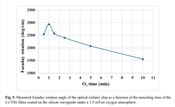
To improve the magneto-optical properties of the sputtered Ce:YIG films, a rapid thermal processing (RTP) step was performed. The thermal treatment was performed in a two-step process: a 725 °C anneal for 9 minutes under vacuum, followed by a 1-minute anneal at the same temperature under a 1.5 mTorr oxygen atmosphere. Figure 5 shows the changes in measured Faraday rotation characteristics as a function of the heat treatment period in the oxygen environment for relatively thick MO films of 48-nm-thick YIG and 387-nm-thick Ce:YIG. Under the given thickness conditions, the vacuum 9-minute and oxygen 1-minute heat treatments produced the best magneto-optical properties, and at this time, a Faraday rotation value of approximately 2940 deg/cm was measured at a wavelength of 1550 nm. Based on these results, the same heat-treatment conditions are applied as those identified as optimal for subsequent device fabrication. For the demonstrated integrated optical isolator device, relatively thin magnetic films of 32-nm-thick YIG and 188-nm-thick Ce:YIG were coated on the silicon waveguides to achieve a low-loss condition. In this case, the same RTP conditions were applied, but the Faraday rotation value decreased slightly to approximately 1905 deg/cm due to the reduced film thickness. This decrease may be attributed to differences in film thickness and suboptimal thermal conditions.
It is important to note that the thermal annealing temperature used in this study is relatively high compared to typical CMOS back-end process limits. To further enhance CMOS compatibility and reduce the thermal budget, alternative crystallization methods such as localized laser annealing might be considered. Laser annealing allows for selective heating of the MO film while minimizing thermal effects on the surrounding silicon photonic structures and has recently been shown as a promising technique for crystallizing Ce:YIG films deposited on non-garnet substrates [32]. The combination of localized laser annealing techniques with a
proper vacuum chamber and oxygen environment, as used in the rapid thermal processes in this research, could offer a feasible pathway to fully CMOS-compatible monolithic integration of magneto-optical isolators.
4.4 Characterization of magneto-optical properties of the Ce:YIG thin films
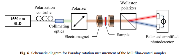
The magneto-optical properties of the Ce:YIG thin film were evaluated using Faraday rotation (FR) measurements. Figure 6 shows the experimental setup used for the FR measurements. A linearly polarized superluminescent laser diode beam at 1550 nm was sent through the MO film sample placed between a pair of electromagnets under an applied external magnetic field, and the polarization rotation of the transmitted light was measured with a Wollaston polarizer and a balanced amplified photodetector.
The measured Faraday rotation curve for the 32-nm-thick YIG and 188-nm-thick Ce:YIG films coated on a silicon wafer is shown in Fig. 7. The saturated Faraday rotation value was 1905 deg/cm at 1550 nm, sufficient to provide the MO effect for the NPS-type optical isolator chip demonstration. Although the measured Faraday rotation value is lower than the maximum
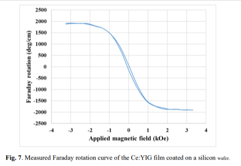
of 2940 deg/cm for the 387-nm-thick Ce:YIG film, the 188-nm-thick Ce:YIG film was chosen to reduce optical loss in the given waveguide geometry because the optical waveguide loss with the MO clad increases as the Ce:YIG film thickness increases in the silicon core and stacked MO film structure. Therefore, in this study, considering the trade-off between Faraday rotation and optical loss, the 188-nm-thick Ce:YIG film was selected to demonstrate an optical isolator chip with low insertion loss.
5. Optical Isolator chip performance.
The performance of optical isolator chips based on silicon waveguides with sputter-coated 32- nm-thick YIG and 188-nm-thick Ce:YIG clad films was characterized by measuring the transmittance spectra of the forward and backward beams through the chips under an external magnetic field of about 1500 Gauss. The measured transmittance spectra are shown in Fig. 8.
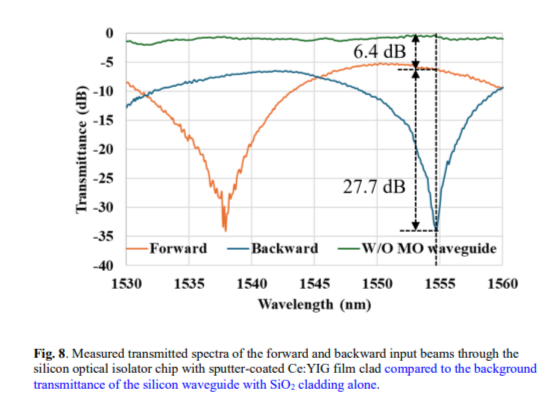
The maximum optical isolation was 27.7 dB, and the minimum insertion loss was 6.4 dB. The 20-dB isolation bandwidth was about 1.1 nm. This result indicates that monolithically integrated silicon-waveguide isolator chips with a sputter-coated Ce:YIG film clad can be successfully operated in photonic integrated circuit applications.
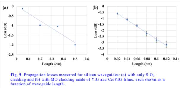
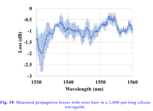
The insertion loss of the fabricated optical isolator chip was determined by measuring the optical propagation losses of its individual waveguide sections. In Fig. 9(a), the measured propagation loss of the silicon waveguide with only SiO2 cladding is shown as a function of waveguide length. The loss was found to be approximately −3.79 dB/cm, which results in about 1.0 dB of loss over the total waveguide length of 2600 μm for the isolator chip, as shown in Fig. 10. Figure 9(b) displays the propagation loss of the MO waveguide section where YIG and Ce:YIG thin films are coated on the silicon waveguide. The measured propagation loss in this MO-clad waveguide region was around −26.68 dB/cm, corresponding to roughly 2.7 dB loss over the 1000 μm-long MO interaction section used in the isolator structure.
Besides the propagation losses in the waveguide sections, the chip includes two multimode interferometers (MMIs) that act as the optical splitter and combiner at both ends of the Mach–
ehnder interferometer setup. The excess loss from both MMIs was estimated at around 0.4 dB.
By combining these contributions, the isolator’s optical insertion loss, excluding the grating couplers, can be estimated. The silicon waveguide section with SiO2 cladding alone contributes approximately 1.0 dB, the waveguide section with MO cladding adds about 2.7 dB, and the MMI structures contribute roughly 0.4 dB of loss. Consequently, the estimated optical insertion loss of the isolator chip is around 4.1 dB.
However, the experimentally measured However, the experimentally measured insertion loss of the isolator chip was 6.4 dB, which exceeds the estimated internal loss. This discrepancy can mainly be attributed to two factors. First, the characteristics of the fabricated grating couplers were not uniform. Their insertion loss and coupling efficiency varied from chip to chip, potentially leading to inaccurate calibration of the grating coupler efficiency when determining the isolator chip’s insertion loss. Second, the fabricated chip did not meet the ideal nonreciprocal phase shift condition required for constructive interference in the forward direction of the Mach-Zehnder interferometer. If the phase shift deviates from the optimal value, some of the optical power may not be fully transferred to the output port, resulting in increased insertion loss.
Further improvements can be made by optimizing the thicknesses of the YIG and Ce:YIG films coated on the silicon waveguide and their thermal treatment conditions. An optimized silicon waveguide design, together with ideal MO film conditions, is essential for maximizing the Faraday rotation properties of the Ce:YIG-film-coated silicon waveguide and for demonstrating compact optical isolator chips.
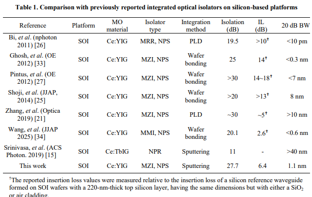
Table 1 summarizes a comparison between the optical isolator chip implemented in this study and representative SOI-based integrated optical isolators previously reported. Previous studies achieved isolation levels of 20-30 dB and operating bandwidths exceeding several nanometers but required relatively limited integration processes such as wafer bonding or PLD. Some studies have reported very low insertion losses in isolator devices fabricated from SOI wafers with a 220-nm-thick top silicon layer. However, these insertion loss values were measured relative to the insertion loss of a silicon reference waveguide with the same dimensions but with either a SiO2 or an air cladding. Isolator devices based on SOI wafers with top MO cladding are effective for TM-mode beams. Unfortunately, silicon waveguides made with SOI wafers having a 220-nm-thick top silicon layer themselves have relatively high propagation loss for TM-mode beams. This is why SOI wafers with a 350-nm-thick top silicon layer were used in our isolator fabrication to reduce propagation loss across the entire waveguide.
This study aimed to demonstrate the feasibility of monolithically integrated MZI-type optical isolator chips with sputter-coated MO film clad. We anticipate that silicon-waveguidebased optical isolator chips with sputter-coated MO films can be further improved for compact, fully integrated PICs. There remains ample room to improve the MO properties of the YIG and Ce:YIG films, as well as the silicon waveguide devices, to achieve such high-performance isolator chips. In this study, have not considered the wideband characteristics of the MZItype optical isolators. The 20-dB isolation bandwidth can also be improved by appropriately
designing the silicon waveguide device and optimizing the MO film conditions.
6. Conclusion
In this study, we experimentally demonstrated an NPS-based integrated optical isolator by directly sputtering MO films onto a silicon waveguide. The YIG buffer and Ce:YIG MO films were sequentially deposited on a silicon waveguide structure fabricated using a standard silicon photonics foundry process. The magneto-optical properties of the Ce:YIG films were optimized via rapid thermal annealing processes.
Numerical analysis of mode confinement and NPS characteristics in TM mode confirmed that an NPS of approximately 65 deg/mm per unit length could be achieved at a waveguide width of 450 nm. In the actual fabrication of the optical isolator device, considering optical loss in the waveguide/MO stack structure, 32 nm YIG and 188 nm Ce:YIG magnetic films were used. The Ce:YIG film exhibited a Faraday rotation of 1905 deg/cm at 1550 nm.
The fabricated optical isolator achieved a maximum isolation of 27.7 dB and an insertion loss of 6.4 dB, with a 20-dB isolation bandwidth of approximately 1.1 nm. These results demonstrate that monolithically integrated optical isolators can be realized on a silicon photonics platform using a mass-producible sputtering process to deposit MO films on silicon waveguide structures. The initial chip performance exhibited relatively high insertion loss and a narrow isolation bandwidth; however, further improvements in high-performance isolator chips can be achieved by optimizing the silicon waveguide structures, the MO film coating, and the thermal treatment conditions. These monolithic optical isolator chips will enable the broad development of photonic integrated-circuit applications.
Funding. Korea Ministry of SMEs and Startups (MSS) (TIPS Program RS-2023-00302394, and RS-2024- 00447487), Basic Science Research Program through the National Research Foundation of Korea funded by the Ministry of Education (RS-2022-NR070869).
Acknowledgment. This work was supported partially by the Startup 1000 Project (micro DIPS #20279476) funded by the Ministry of SMEs and Startups through Seoul National University − System Semiconductor Industry Promotion Center. K.H. Kim thanks Mr. Jasper Leong at CompoundTek, Pte Ltd. for arranging collaborative foundry services.
Disclosures. The authors declare no conflicts of interest.
Data availability. Data underlying the results presented in this paper are not publicly available at this time but may be obtained from the authors upon reasonable request Supplementary Document. See Supplement 1 for supporting content.
References
1. S. Wang, M. L. Shah, and J. D. Crow, “Wave Propagation in Thin-Film optical Waveguides Using Gyrotropic and Anisotorpic Materials as Substrates,” IEEE J. Quantum Electronics QE-8(2), 212‒216 (1972).
2. F. Auracher and H. H. Witte, “A new design for an integrated optical isolator,” Opt. Commun. 13, 435‒438 (1975).
3. L. Fan, L. T. Varghese, J. Wang, et al., “Silicon optical diode with 40 dB nonreciprocal transmission,” Opt. Lett. 38(8), 1259‒1261 (2013).
4. K. Abdelsalam, T. Li, J. B. Khurgin, et al., “Linear isolators using wavelength conversion”. Optica 7(3), 209‒ 213 (2020).
5. Y. Yu, Y. Chen, H. Hu, et al., “Nonreciprocal transmission in a nonlinear photonic-crystal Fano structure with broken symmetry,” Laser Photonics Rev. 9(2), 241‒247 (2015).
6. P. Dong and C. Gui, “Observation of nonreciprocal transmission in binary phase-shift keying modulation using traveling-wave Mach–Zehnder modulators,” Opt.
Lett. 41(12), 2723‒2726 (2016).
7. H. Tian, J. Liu, A. Siddharth, et al., “Magnetic-free silicon nitride integrated optical isolator,” Nat. Photon. 15, 828‒836 (2021).
8. K. Fang, J. Luo, A. Metelmann, et al., “Generalized non-reciprocity in an optomechanical circuit via synthetic magnetism and reservoir engineering,” Nat. Physics 13, 465‒472 (2017).
9. H. Cheng, Y. Zhou, F. Ruesink, et al., “A terahertz-bandwidth non-magnetic isolator,” Nat. Photon. 19, 533‒ 539 (2025).
10. D. B. Sohn, O. Őrsel, and G. Bahl, “Electrically driven optical isolation through phonon-mediated photonic Autler–Townes splitting,” Nat. Photon. 15, 822‒827 (2021).
11. Y. Choi, C. Hahn, J. W. Yoon, et al., “Extremely broadband, on-chip optical nonreciprocity enabled by mimicking nonlinear anti-adiabatic quantum jumps near exceptional points,” Nat. Commun. 8, 14154‒1~9 (2017).
12. R. Wolfe, J. Hegarty, J. F. Dillon. Jr., et al., “Magneto-optic Waveguide Isolators Based on Laser Annealed (Bi, Ga) YIG Films,” IEEE Trans. on Magnetics MAG-21(5), 1647‒1650 (1985).
13. M. Levy, R. M. Osgood, Jr., H. Hegde, et al., “Integrated Optical Isolators with Sputter-Deposited Thin-Film Magnets,” IEEE Photon. Technol. Lett. 8(7), 903‒905 (1996).
14. B. M Holmes and D. C. Hutchings, “Demonstration of quasi-phase-matched nonreciprocal polarization rotation in III-V semiconductor waveguides incorporating magneto-optic upper claddings,” Appl. Phys. Lett. 88, 061116 (2006).
15. K. Srinivasan, C. Zhgang, P. Dulal, et al., “High-Gyrotropy Seedlayer-Free Ce:TbIG for Monolithic LaserMatched SOI Optical Isolators,” ACS Photon. 6, 2455‒461 (2019).
16. T. Mizumoto and Y. Naito, “Nonreciprocal Propagation Characteristics of YIG Thin Film,” IEEE Trans. on Microwave Theory & Techniq. MTT-30(6), 922‒925 (1982).
17. T. Mizumoto, S. Mashimo, T. Ida, et al., “In-Plane Magnetized Rare Earth Iron Garnet for a Waveguide Optical Isolator Employing Nonreciprocal Phase Shift,” IEEE Trans. on Magnetics MAG-29(6), 3417‒3419 (1993).
18. G. Dushaq, S. Serunjogi, S. R. Tamalampudi, et al., “Non-reciprocal response in silicon photonic resonators integrated with 2D CuCrP2S6 at short-wave infrared,” Light Sci. & Appl. 14, 157‒1~13 (2025).
19. S. Liu, Y. Shoji, and T. Mizumoto, “TE-mode magneto-optical isolator based on an asymmetric microring resonator under a unidirectional magnetic field,” Opt. Express 30(6), 9934‒9943 (2022).
20. S. Ghosh, S. Keyvaninia, Y. Shirato, et al., “Optical Isolator for TE Polarized Light Realized by Adhesive Bonding of Ce:YIG on Silicon-on-Insulator Waveguide Circuits,” IEEE Photon. J. 5(3), 6601108‒1~8 (2013).
21. Y. Zhang, et al., “Monolithic integration of broadband optical isolators for polarization-diverse silicon photonics,” Optica 6(4), 473‒8 (2019).
22. G. Portela, Y. Ni, K. Sato, et al., “Ultra-Compact Photonic Isolator Based on Bias-Free Magneto-Optical Thin Films,” Prog. in Electromagn. Res. 182, 77‒83 (2025).
23. Z. Wei, Y. Yang, D. Wu, et al., “Recent development of magneto-optical thin films and integrated photonic devices,” J. of Mater. Chem. C 13, 12628 (2025).
24. Y. Shoji, I-W. Hsieh, R. M. Osgood, et al., “Polarization-Independent Magneto-Optical Waveguide Isolator Using TM-Mode Nonreciprocal Phase Shift,” J. Lightwave Technol. 25(10), 3108‒3113 (2007).
25. Y. Shoji, Y. Shirao, and T. Mizumoto, “Silicon Mach-Zehnder interferometer optical isolator having 8 nm bandwidth for over 20 dB isolation,” Jpn. J. Appl. Phys. 53, 022202 (2014).
26. L. Bi, J. Hu, P. Jiang, et al., “On-chip optical isolation in monolithically integrated non-reciprocal optical resonators,” Nat. Photon. 5, 758‒762 (2011).
27. P. Pintus, D. Huang, P. A. Morton, et al., “Broadband TE Optical Isolators and Circulators in Silicon Photonics Through Ce:YIG Bonding,” J. Lightwave Technol. 37(5), 1463‒1472 (2019).
28. S. Liu, Y. Shoji, and T. Mizumoto, “Mode-evolution-based TE mode magneto-optical isolator using asymmetric adiabatic tapered waveguides,” Optics Express 29(15), 22838‒22846 (2021).
29. S. Liu, D. Minemura, and Y. Shoji, “Silicon-based integrated polarization-independent magneto-optical isolator,” Optica 10(3), 373‒378 (2023).
30. D. Minemura, R. Kou, Y. Sutoh, et al., Compact magneto-optical isolator by µ-transfer printing of magnetooptical single-crystal film on silicon waveguides,” Optics Express 31(17), 27821‒27828 (2023).
31. Y. Yang, T. Zhang, D. Wu, et al., “Europium-substituted cerium iron garnet thin films for silicon-integrated nonreciprocal photonic device applications,” APL Mater. 13, 051109 (2025).
32. H. Miyashita et al., Vacuum laser annealing of magnetooptical cerium-substituted yttrium iron garnet films, Optical Materials 146, 114530 (2023).
33. S. Ghosh, J. Van Campenhout, F. De Smet, et al., “Ce:YIG/SOI waveguide optical isolator,” Opt. Express 20(2), 1839‒1848 (2012).
34. J. Wang, M. Okano, and Y. Shoji, “Low-loss magneto-optical isolator using a tapered multimode interferometer for TE-mode input on silicon photonic platforms,” Jpn. J. Appl. Phys. 64, 072004 (2025)